| CPC H01L 21/76883 (2013.01) [H01L 21/76802 (2013.01); H01L 21/76886 (2013.01); H01L 23/528 (2013.01); H01L 23/5226 (2013.01); H01L 23/53233 (2013.01)] | 20 Claims |
|
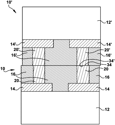
1. A method of forming an electrical interconnect in a via hole of an electrical device, the method comprising:
depositing a Sn layer in the via hole;
depositing a Cu layer atop and in contact with the Sn layer; and
heating the Sn layer and the Cu layer such that the Sn and Cu layers diffuse together to form a Cu3Sn interconnect in the via hole;
wherein during the heating, a diffusion front between the Sn and Cu layers moves in a direction toward the Cu layer initially deposited;
wherein the heating causes Cu atoms in the Cu layer to diffuse across the diffusion front into the Sn layer to form the Cu3Sn interconnect;
wherein the heating causes vacancy diffusion and the formation of Kirkendall voids at an interface between the formed Cu3Sn interconnect and remaining Cu layer; and
wherein the method is carried out such that the Kirkendall voids are at an upper portion of the via hole or above an upper surface of a layer in which the via hole is formed; and
further comprising: removing the Kirkendall voids and the remaining Cu layer.
|