| CPC H01L 21/6835 (2013.01) [B29C 59/026 (2013.01); G03F 7/0002 (2013.01); H01L 21/306 (2013.01); H01L 21/568 (2013.01); H01L 21/7806 (2013.01); H01L 23/3171 (2013.01); H01L 24/24 (2013.01); H01L 24/29 (2013.01); H01L 24/75 (2013.01); H01L 24/97 (2013.01); H01L 25/0753 (2013.01); H01L 25/50 (2013.01); H05K 1/111 (2013.01); H01L 2221/68368 (2013.01); H01L 2221/68381 (2013.01); H01L 2224/95001 (2013.01); H01L 2224/951 (2013.01); H01L 2224/95136 (2013.01); H01L 2924/1815 (2013.01)] | 20 Claims |
|
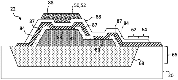
1. A component source wafer, comprising a source wafer having native micro-transfer printable components disposed on or in the source wafer over an etchable sacrificial layer, each of the micro-transfer printable components comprising a device and an ablation layer disposed on a side of the device opposite the source wafer, wherein the source wafer is a semiconductor wafer on which the native micro-transfer printable components have been constructed.
|