| CPC H01L 21/4857 (2013.01) [G06N 10/00 (2019.01); H01L 23/49822 (2013.01); H01L 33/06 (2013.01)] | 37 Claims |
|
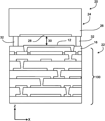
1. A method of fabricating a carrier chip for distributing signals among circuit elements of a quantum computing device, the method comprising:
providing a multilayer wiring stack, the multilayer wiring stack comprising alternating layers of dielectric material and wiring;
bonding a capping layer to the multilayer wiring stack, wherein the capping layer comprises a single crystal silicon dielectric layer;
forming a via hole within the capping layer, wherein the via hole extends to a first wiring layer of the multilayer wiring stack;
forming an electrically conductive via within the via hole and electrically coupled to the first wiring layer; and
forming a circuit element on a surface of the capping layer, wherein the circuit element is directly electrically coupled to the electrically conductive via.
|