| CPC H01L 21/31053 (2013.01) [H01L 21/0223 (2013.01); H01L 21/02252 (2013.01); H01L 21/76814 (2013.01)] | 20 Claims |
|
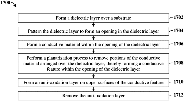
1. A method comprising:
forming a dielectric layer over a substrate;
patterning the dielectric layer to form an opening in the dielectric layer;
forming a conductive material within the opening of the dielectric layer;
performing a planarization process to remove portions of the conductive material arranged over the dielectric layer thereby forming a conductive feature within the opening of the dielectric layer; and
performing a post-planarization drying process, wherein the post-planarization drying process uses a mixture of a drying solution, a reducing agent, and an inhibitor compound,
wherein the drying solution is configured to remove any cleaning solutions present from prior cleaning processes on the dielectric layer and the conductive feature,
wherein the reducing agent is configured to reduce an oxidation compound comprising the conductive material and oxygen,
wherein the inhibitor compound is configured to bind to a topmost surface of the conductive feature,
wherein an anti-oxidation layer is formed on an upper surface of the conducive feature during the post-planarization drying process.
|