US 11,854,809 B2
Manufacturing method of a semiconductor device with efficient edge structure
Edoardo Zanetti, Valverde (IT); Simone Rascuna', Catania (IT); Mario Giuseppe Saggio, Aci Bonaccorsi (IT); Alfio Guarnera, Trecastagni (IT); Leonardo Fragapane, Catania (IT); and Cristina Tringali, Augusta (IT)
Assigned to STMICROELECTRONICS S.r.l., Agrate Brianza (IT)
Filed by STMICROELECTRONICS S.r.l., Agrate Brianza (IT)
Filed on Dec. 5, 2022, as Appl. No. 18/061,795.
Application 18/061,795 is a continuation of application No. 17/244,393, filed on Apr. 29, 2021, granted, now 11,545,362.
Application 17/244,393 is a continuation of application No. 16/209,680, filed on Dec. 4, 2018, granted, now 11,018,008, issued on May 25, 2021.
Claims priority of application No. 102017000140373 (IT), filed on Dec. 5, 2017.
Prior Publication US 2023/0099610 A1, Mar. 30, 2023
Int. Cl. H01L 21/04 (2006.01); H01L 21/285 (2006.01); H01L 29/872 (2006.01); H01L 29/66 (2006.01); H01L 29/16 (2006.01); H01L 29/78 (2006.01); H01L 29/06 (2006.01)
CPC H01L 21/046 (2013.01) [H01L 21/0495 (2013.01); H01L 21/28537 (2013.01); H01L 29/0619 (2013.01); H01L 29/0661 (2013.01); H01L 29/1608 (2013.01); H01L 29/6606 (2013.01); H01L 29/66068 (2013.01); H01L 29/66143 (2013.01); H01L 29/66734 (2013.01); H01L 29/7811 (2013.01); H01L 29/7813 (2013.01); H01L 29/872 (2013.01); H01L 29/8725 (2013.01)] 18 Claims
OG exemplary drawing
 
1. A structure, comprising:
a substrate;
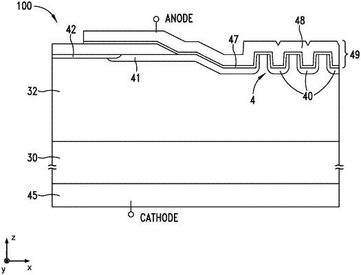
a drift layer on the substrate;
a first trench in the drift layer, the first trench including a transition region and a side wall, the side wall having a first slope that is steeper than a second slope of the transition region; and
an edge-termination structure on the drift layer;
an anode metallization on the first trench.