| CPC G11C 7/12 (2013.01) [G11C 5/063 (2013.01); G11C 7/22 (2013.01)] | 13 Claims |
|
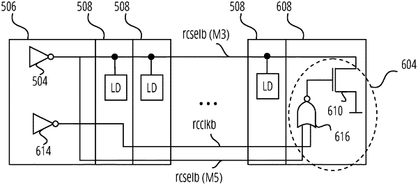
1. A circuit comprising:
a signal driver to generate a signal at a first end of a signal path;
the signal path splitting into a first route and a second route, wherein the first route is loaded to an extent that, in the absence of the second route, degrades a slew rate of the signal at a second end of the signal path;
the second route being lightly loaded or unloaded relative to the first route;
a transistor configured to pull down the signal on the first route;
a pulse shaping circuit coupling the first route to the second route at the second end of the signal path; and
wherein the pulse shaping circuit comprising a NAND combination of the second route and a timing control signal coupled to a gate of the transistor.
|