US 11,854,658 B2
Memory buffer with data scrambling and error correction
Christopher Haywood, Cary, NC (US); and David Wang, Westlake Village, CA (US)
Assigned to Rambus Inc., San Jose, CA (US)
Filed by Rambus Inc., San Jose, CA (US)
Filed on Mar. 16, 2022, as Appl. No. 17/696,818.
Application 17/696,818 is a continuation of application No. 16/831,121, filed on Mar. 26, 2020, granted, now 11,282,552.
Application 16/831,121 is a continuation of application No. 15/978,344, filed on May 14, 2018, granted, now 10,607,669, issued on Mar. 31, 2020.
Application 15/978,344 is a continuation of application No. 14/923,345, filed on Oct. 26, 2015, granted, now 9,972,369, issued on May 15, 2018.
Application 14/923,345 is a continuation of application No. 13/791,124, filed on Mar. 8, 2013, granted, now 9,170,878, issued on Oct. 27, 2015.
Application 13/791,124 is a continuation in part of application No. 13/619,692, filed on Sep. 14, 2012, granted, now 8,880,790, issued on Nov. 4, 2014.
Application 13/619,692 is a continuation in part of application No. 13/359,877, filed on Jan. 27, 2012, granted, now 8,694,721, issued on Apr. 8, 2014.
Claims priority of provisional application 61/682,412, filed on Aug. 13, 2012.
Claims priority of provisional application 61/661,549, filed on Jun. 19, 2012.
Claims priority of provisional application 61/691,736, filed on Aug. 21, 2012.
Claims priority of provisional application 61/473,889, filed on Apr. 11, 2011.
Prior Publication US 2022/0277780 A1, Sep. 1, 2022
Int. Cl. G11C 7/10 (2006.01); G06F 11/10 (2006.01); G06F 11/07 (2006.01); G11C 29/52 (2006.01); G11C 29/04 (2006.01); G11C 5/04 (2006.01)
CPC G11C 7/1072 (2013.01) [G06F 11/073 (2013.01); G06F 11/0778 (2013.01); G06F 11/0787 (2013.01); G06F 11/1044 (2013.01); G06F 11/1048 (2013.01); G06F 11/1068 (2013.01); G11C 7/1006 (2013.01); G06F 11/1008 (2013.01); G11C 5/04 (2013.01); G11C 29/52 (2013.01); G11C 2029/0411 (2013.01)] 17 Claims
OG exemplary drawing
 
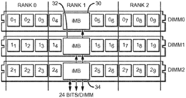
7. A method of operation of a memory buffer circuit comprising:
receiving, by a memory interface of the memory buffer circuit, at least a portion of a scrambled data word from a first plurality of volatile memory devices in a first memory module;
de-scrambling, by a processing engine of the memory buffer circuit, the portion of the scrambled data word into an unscrambled data word using a pseudo-random process and state information comprising at least one of an address or a bank address; and
transferring, by a host interface of the memory buffer circuit, the unscrambled data word to a host controller in response to a data access request received from the host controller.