| CPC G11C 5/147 (2013.01) [G05F 1/462 (2013.01); G05F 1/575 (2013.01); G05F 1/59 (2013.01)] | 23 Claims |
|
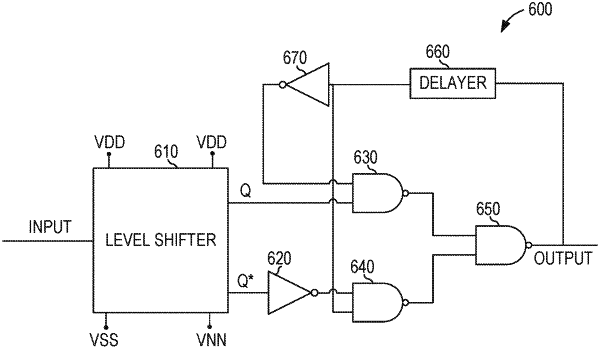
1. A semiconductor device comprising:
a level shifter that:
receives an input in a first power domain;
provides a first output in a second power domain; and
provides a second output in the second power domain; and
a ramp selection circuit that:
receives as input the first output and the second output from the level shifter;
inverts the second output; and
provides one of the first output and the inverted second output as an output of the ramp selection circuit.
|