| CPC G11C 11/4076 (2013.01) [G06F 1/08 (2013.01); G06F 1/10 (2013.01); G06F 3/0604 (2013.01); G06F 3/0659 (2013.01); G06F 3/0671 (2013.01)] | 20 Claims |
|
1. A memory controller, comprising:
a command queue including a plurality of entries for holding incoming memory access commands;
an arbiter for selecting commands from the command queue for dispatch to a memory; and
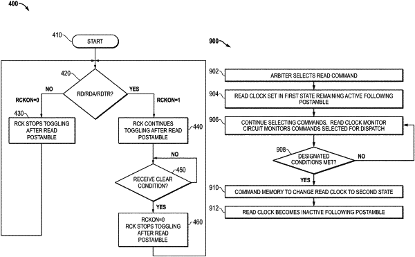
a read clock control circuit for monitoring read commands selected for dispatch to the memory, and responsive to a designated condition, commanding the memory to change a state of a read clock from a first state in which the read clock remains active following a postamble period for a read command, to a second state in which the read clock becomes inactive following the postamble period.
|