| CPC G06F 3/0611 (2013.01) [G06F 3/068 (2013.01); G06F 3/0625 (2013.01); G06F 3/0626 (2013.01); G06F 3/0647 (2013.01); G06F 3/0653 (2013.01); G06F 3/0659 (2013.01); G11C 11/005 (2013.01); G11C 11/221 (2013.01); G11C 11/2259 (2013.01); G11C 11/404 (2013.01); G11C 11/4096 (2013.01); G11C 14/0027 (2013.01); H01L 23/528 (2013.01); H01L 28/55 (2013.01); H10B 12/03 (2023.02); H10B 12/30 (2023.02); H10B 53/30 (2023.02); G11C 11/2273 (2013.01); G11C 2207/2245 (2013.01)] | 19 Claims |
|
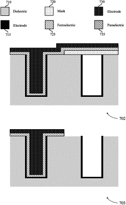
1. A method of forming a memory apparatus, comprising:
forming an array of recesses in a substrate;
forming a first conductive material on a surface of two or more recesses of the array;
forming a first mask material over a second recess before forming a first memory element material; and
forming the first memory element material comprising a ferroelectric material in a first recess of the array, wherein the first memory element material is coupled to the first conductive material in the first recess;
forming a second mask material over the first recess before forming a second memory element material; and
forming the second memory element material comprising a paraelectric material in the second recess of the array, wherein the second memory element material is coupled to the first conductive material in the second recess.
|