| CPC G06F 3/041 (2013.01) [G06F 2203/04103 (2013.01)] | 22 Claims |
|
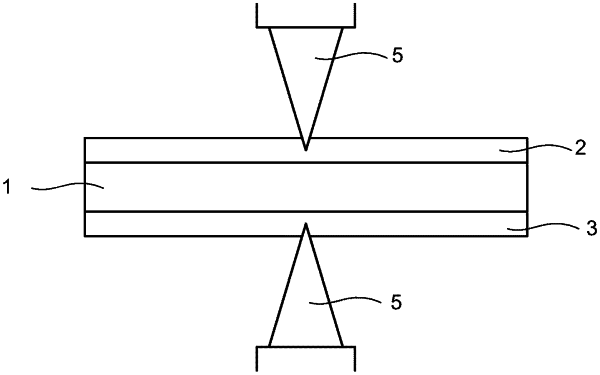
1. A method of manufacturing a transparent conductive film for a touch sensitive panel, comprising:
providing a layered structure comprising a plurality of homogeneous layers which include at least a first transparent conductive layer, a second transparent conductive layer, and a transparent support substrate between the first transparent conductive layer and the second transparent conductive layer, the transparent support substrate being the thickest layer of the layered structure;
forming an electrode pattern in the first transparent conductive layer by laser ablation of the first transparent layer by a laser beam incident on the first transparent layer from a side of the transparent support substrate on which the first transparent layer is provided; wherein
the laser beam and transparent support substrate are configured such that during laser ablation, the material and thickness of the transparent support substrate are such that the laser beam energy density is reduced by 75% or more by absorption by the transparent support substrate;
wherein the first and/or second transparent conductive layers have an ablation threshold of from 0.5 Jcm−2 to 1 Jcm−2.
|