| CPC G06F 13/4282 (2013.01) [G06F 9/30134 (2013.01); G06F 13/28 (2013.01); G06F 13/4072 (2013.01)] | 20 Claims |

|
1. A processing system comprising:
a transmission terminal configured to provide a transmission signal;
a reception terminal (RX) configured to receive a reception signal;
a microprocessor programmable via software instructions;
a memory controller configured to be connected to a memory;
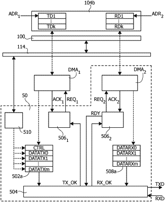
a communication system connecting the microprocessor, the memory controller and a serial communication interface; and
the serial communication interface, supporting a controller area network flexible data-rate (CAN FD) Light mode of operation and a universal asynchronous receiver/transmitter (UART) mode of operation, wherein the serial communication interface comprises:
a control register configured to store data identifying a clock scaling factor, data identifying a requested number of bits and data identifying a mode of operation, the mode of operation indicating the CAN FD Light mode of operation or the UART mode of operation, wherein the control register is programmable via the microprocessor;
a clock management circuit configured to receive a clock signal and generate a down-scaled clock signal as a function of the clock scaling factor stored to the control register;
a transmission shift register configured to, when a transmission enable signal is asserted, generate the transmission signal by sequentially providing a content of the transmission shift register in response to the down-scaled clock signal, wherein the processing system is adapted to selectively transfer data from the microprocessor to the transmission shift register;
a transmission control circuit configured to:
receive a start of transmission signal requesting transmission of data;
in response to the start of transmission signal, assert the transmission enable signal;
when the transmission enable signal is asserted, increase a transmission count value in response to the down-scaled clock signal;
determine whether the transmission count value reaches the requested number of bits; and
in response to determining that the transmission count value reaches the requested number of bits, de-assert the transmission enable signal;
a reception shift register configured to, when a reception enable signal is asserted, sequentially add a logic level of the reception signal to a content of the reception shift register in response to the down-scaled clock signal, wherein the processing system is adapted to selectively transfer data from the reception shift register to the microprocessor; and
a reception control circuit configured to:
detect a falling edge in the reception signal;
in response to detecting the falling edge in the reception signal, assert the reception enable signal;
determine whether the data stored to the control register indicate the CAN FD Light mode of operation or the UART mode of operation;
in response to determining that the data stored to the control register indicate the CAN FD Light mode of operation:
when the reception enable signal is asserted and the reception signal is set to high, increase a first reception count value in response to the down-scaled clock signal;
reset the reception count value each time the reception signal is set to low;
determine whether the reception count value reaches eight; and
in response to determining that the reception count value reaches eight, de-assert the reception enable signal; and
in response to determining that the data stored to the control register indicate the UART mode of operation:
when the reception enable signal is asserted, increase a second reception count value in response to the down-scaled clock signal;
determine whether the reception count value reaches the requested number of bits; and
in response to determining that the reception count value reaches the requested number of bits stored to the control register, de-assert the reception enable signal.
|