| CPC G06F 1/3203 (2013.01) [G06F 1/04 (2013.01); H02M 3/156 (2013.01); H04L 7/0008 (2013.01); G06F 1/10 (2013.01); G06F 1/26 (2013.01)] | 8 Claims |
|
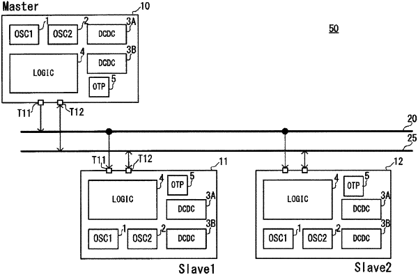
1. A semiconductor device system, comprising:
a first semiconductor device as a master, the first semiconductor device including a clock terminal configured to at least one of output or receive a first clock,
a data terminal configured to at least one of output or receive data in synchronization with the first clock,
wherein,
the synchronized data is output from the data terminal, and
the first clock is output from the clock terminal irrespective of whether or not data transfer of the synchronized data is being executed; and
a second semiconductor device having a configuration same as the first semiconductor device, as a slave, wherein
the first semiconductor device as the master outputs the first clock, and
the first clock is input to the second semiconductor device which is the slave.
|