| CPC G02B 6/1225 (2013.01) [G02B 2006/1213 (2013.01); G02B 2006/12104 (2013.01)] | 15 Claims |
|
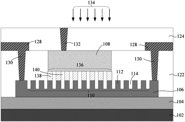
1. A semiconductor device comprising:
a substrate;
a photonic component arranged above the substrate;
a first bottom reflector arranged above the substrate and positioned below the photonic component; and
a second bottom reflector arranged vertically between the first bottom reflector and the photonic component, wherein the first bottom reflector and the second bottom reflector have a plurality of grating structures configured to reflect electromagnetic waves towards the photonic component, and wherein the grating structures in the first bottom reflector have top surfaces, and the grating structures in the second bottom reflector is directly on the top surfaces of the grating structures in the first bottom reflector.
|