| CPC G02B 5/1814 (2013.01) [G01S 7/4814 (2013.01); G01S 7/4817 (2013.01); G02B 27/42 (2013.01); G01S 17/89 (2013.01)] | 10 Claims |
|
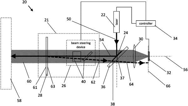
1. An optoelectronic device, comprising:
an output optic, having one or more optical surfaces;
a light source configured to emit a beam of light;
a mirror comprising:
a central reflective region positioned to reflect the beam from the light source through the output optic along an axis toward a target scene; and
a peripheral region having a width of at least 1 mm surrounding the central reflective region, and having an optical density that decreases in a radial direction over the width;
an optical sensor; and
light collection optics, which are positioned to receive the light returned from the target scene through the output optic and transmitted through a collection aperture surrounding the mirror and to focus the collected light along the axis onto the optical sensor.
|