US 11,852,701 B2
Defect centre-based sensor
Angelo Frangeskou, Coventry (GB); Gavin Morley, Coventry (GB); Ben Green, Coventry (GB); Ben Breeze, Coventry (GB); Matthew Dale, Coventry (GB); and Rajesh Patel, Coventry (GB)
Assigned to The University of Warwick, Coventry (GB)
Appl. No. 17/427,127
Filed by The University of Warwick, Coventry (GB)
PCT Filed Jan. 29, 2020, PCT No. PCT/GB2020/050207
§ 371(c)(1), (2) Date Jul. 30, 2021,
PCT Pub. No. WO2020/157497, PCT Pub. Date Aug. 6, 2020.
Claims priority of application No. 1901277 (GB), filed on Jan. 30, 2019.
Prior Publication US 2022/0146605 A1, May 12, 2022
Int. Cl. G01V 3/00 (2006.01); G01R 33/24 (2006.01); G01R 33/44 (2006.01); G02B 6/32 (2006.01); G02B 6/42 (2006.01)
CPC G01R 33/24 (2013.01) [G01R 33/445 (2013.01); G02B 6/32 (2013.01); G02B 6/4204 (2013.01)] 20 Claims
OG exemplary drawing
 
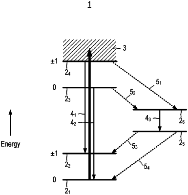
1. A defect centre-based sensor comprising:
instrumentation which includes:
a generator for causing excitation in an active element; and
a detector for measuring a transition in the active element, wherein the generator is an optical source and/or the detector is an optical detector;
an optical waveguide; and
a sensor head in communication with the source and/or the detector via the optical waveguide, the sensor head housing:
the active element having at least one defect centre; and
a signal delivery arrangement arranged to optically couple the optical waveguide to the active element.