| CPC G01R 31/31725 (2013.01) [G01R 31/31721 (2013.01)] | 20 Claims |
|
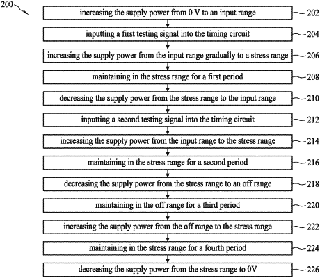
17. A circuit screening method, comprising:
operating in a first input stage, in which a first testing signal is inputted into a target circuit under test, a supply voltage, whose voltage level locates in an input range, is provided to the target circuit under test, and a clock signal having a first profile is provided to the target circuit under test;
operating in a second input stage after the first input stage, in which a second testing signal different from the first testing signal is inputted into the test target circuit under test, and the supply voltage, whose voltage level relocates in the input range, is provided to the test target circuit under test, and a clock signal having a second profile different from the first profile is provided to the target circuit under test;
wherein the first profile and the second profile has a phase difference.
|