| CPC G01C 19/5712 (2013.01) [G01C 19/5755 (2013.01); G01C 19/5769 (2013.01)] | 51 Claims |
|
1. A MEMS motion sensor comprising:
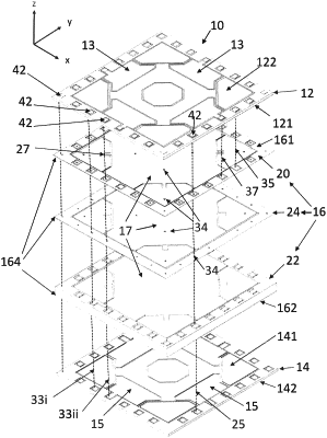
an electrically conductive MEMS silicon-on-insulator (SOI) wafer including an insulating layer separating a device layer from a handle layer, the MEMS SOI wafer having a first side and a second side and including an outer frame, a proof mass and a plurality of flexible springs suspending the proof mass relative to the outer frame and enabling the proof mass to move relative to the outer frame along mutually orthogonal x, y and z axes, the plurality of springs formed in the device layer;
an electrically conductive silicon top cap wafer and an electrically conductive silicon bottom cap wafer respectively bonded to the first side and the second side of the MEMS SOI wafer such that the top cap wafer, the bottom cap wafer and the outer frame of the MEMS SOI wafer define a cavity for housing the proof mass;
a plurality of top cap wafer electrodes and a plurality of bottom cap wafer electrodes that are respectively positioned with the top cap wafer and the bottom cap wafer, the electrodes forming capacitors with the proof mass that are configured to detect at least one of translational and rotational motion of the proof mass, wherein a detected rotational motion includes an angular motion of the proof mass about at least one of the x, y, and z axes;
a plurality of insulated conducting pathways, each insulated conducting pathway conducting signals through at least a portion of each of the silicon top cap wafer, the MEMS SOI wafer, and the silicon bottom cap wafer; and
a first set of electrical contacts on a top surface of the top cap wafer and connected to the plurality of top cap wafer electrodes, a second set of electrical contacts on the top surface of the top cap wafer being connected to the bottom cap wafer electrodes via at least one of the plurality of insulated conducting pathways, and a third set of electrical contacts connected to the proof mass.
|