| CPC G01B 11/303 (2013.01) [G01N 21/93 (2013.01); G01N 21/9501 (2013.01)] | 8 Claims |
|
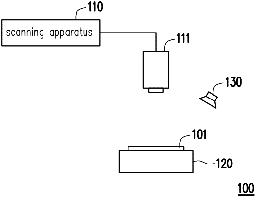
1. A wafer inspection method, adapted for an electronic apparatus comprising a processor, the wafer inspection method comprising:
receiving scanning information of at least one wafer, wherein the scanning information is formatted as a pixel array for forming an image, the pixel array comprising a plurality of pixels and a plurality of haze values;
dividing the image into a plurality of information blocks according to a unit block;
performing a calculation on the plurality of haze values included in each of the plurality of information blocks to obtain a statistical value, and setting the statistical value as a feature value of each of the plurality of information blocks;
equidistantly separating a value range formed by a haze upper threshold and a haze lower threshold according to a set value to generate a plurality of sub-haze values for dividing the value range, and setting each of the sub-haze values to correspond to a color value, wherein in a same batch process test mode and a multi-batch process test mode, the haze upper threshold is set according to a default upper threshold, and the haze lower threshold is set according to a default lower threshold; and
converting the feature value to a corresponding color value by finding one of the sub-haze values corresponding to the feature value of each of the plurality of blocks and extracting the color value corresponding to the found sub-haze value, and generating a color image corresponding to the at least one wafer according to the color value converted from the feature value, wherein the color image displays a texture of the at least one wafer.
|