| CPC C23C 16/45553 (2013.01) [C23C 16/325 (2013.01); C23C 16/36 (2013.01); C23C 16/45538 (2013.01); C23C 16/50 (2013.01); C23C 16/4408 (2013.01); H01L 21/76829 (2013.01)] | 21 Claims |
|
1. A method of forming a dielectric film comprising silicon and carbon onto at least a surface of a substrate, the method comprising the steps of:
a. providing a substrate in a reactor;
b. introducing into the reactor at least one silacycloalkane precursor selected from the group consisting of compounds represented by the structure of Formula IA and compounds represented by the structure of Formula IB:
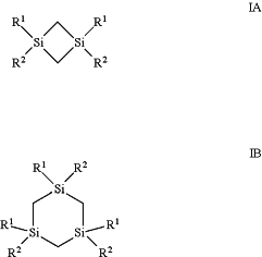 wherein R1 is selected from the group consisting of hydrogen, a linear or branched C1 to C10 alkyl group, a cyclic C3 to C10 alkyl group, a linear or branched C2 to C10 alkenyl group, and a linear or branched C2 to C10 alkynyl group; and R2 is selected from the group consisting of a linear or branched C2 to C6 alkenyl group, a linear or branched C2 to C6 alkynyl group, and a cyclic C3 to C10 alkyl group, wherein the at least one silacycloalkane precursor reacts on at least a portion of the surface of the substrate to provide a chemisorbed layer;
c. purging the reactor with a purge gas;
d. introducing a plasma containing source and an inert gas into the reactor to react with at least a portion of the chemisorbed layer and provide at least one reactive site, wherein the plasma is generated at a power density ranging from about 0.01 to about 1.5 W/cm2; and
e. optionally purging the reactor with an inert gas; and wherein the steps b through e are repeated until a desired thickness of the dielectric film is obtained.
|