| CPC C23C 14/046 (2013.01) [C23C 14/042 (2013.01); C23C 14/225 (2013.01); C23C 14/3407 (2013.01); C23C 14/3464 (2013.01); G02B 6/132 (2013.01); G02B 27/0172 (2013.01); G02B 27/1073 (2013.01); G02B 2027/0178 (2013.01)] | 20 Claims |
|
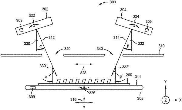
1. A method for encapsulating gratings of a waveguide combiner by asymmetric selective physical vapor deposition (PVD), comprising:
providing a first stream of a first material from a first PVD source towards the waveguide combiner, the waveguide combiner includes an input coupling grating and an output coupling grating, the input coupling grating has at least a first fin structure and a second fin structure, the first stream provided in a first direction to one or more surfaces of a first fin structure and at a first non-perpendicular angle relative to the waveguide combiner;
depositing the first material on the one or more surfaces of the first fin structure, the deposition of the first material forming a first protrusion extending laterally from the first fin structure;
providing a second stream of a second material from a second PVD source towards one or more surfaces of the second fin structure of the input coupling grating, the second stream provided in a second direction and at a second non-perpendicular angle relative to the waveguide combiner; and
depositing the second material on the one or more surfaces of the second fin structure, the deposition of the second material forming a second protrusion extending laterally from the second fin structure, the second protrusion converging with the first protrusion to form an encapsulation layer over the first and second fin structures of the input coupling grating.
|