| CPC B81B 3/0072 (2013.01) [B60T 1/065 (2013.01); B60T 8/17 (2013.01); B60T 8/171 (2013.01); G01L 1/18 (2013.01); G01L 3/00 (2013.01); G01L 9/06 (2013.01); B81B 2201/0264 (2013.01); B81B 2201/0292 (2013.01); B81B 2203/0127 (2013.01); B81B 2203/0315 (2013.01)] | 20 Claims |
|
1. A device, comprising:
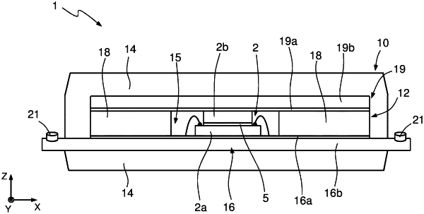
a micromechanical sensing structure configured to provide an electrical detection quantity as a function of a load, the micromechanical sensing structure comprising a first die comprising a semiconductor material, the first die comprising sensing elements integrated in the first die for sensing the load; and
a package enclosing the micromechanical sensing structure and providing a mechanical and electrical interface with respect to an external environment, wherein the package comprises:
a housing structure comprising a cavity, the first die disposed within the cavity and leaving a residual cavity laterally surrounding the first die; and
a package coating that coats, at least in part, the housing structure, the package coating comprising a mechanical interface configured to transfer, in a uniform manner, the load on the housing structure and on the micromechanical sensing structure, wherein the housing structure comprises a deformable layer interposed and in contact between the micromechanical sensing structure and the package coating, and wherein the deformable layer completely closes the cavity at a top surface of the cavity facing away from the micromechanical sensing structure, and defines a mechanical-coupling interface.
|