| CPC B41J 2/33535 (2013.01) [B41J 2/335 (2013.01); B41J 2/3353 (2013.01); B41J 2/3359 (2013.01); B41J 2/33505 (2013.01); B41J 2/345 (2013.01)] | 18 Claims |
|
1. A thermal print head, comprising:
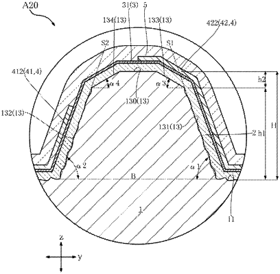
a substrate, having a main surface that faces a thickness direction and a convex portion that protrudes from the main surface and extends along a main scanning direction, wherein the substrate includes a semiconductor material;
a resistor layer, including a plurality of heat generating portions arranged in the main scanning direction and located on the convex portion; and
a wiring layer, conducted to the plurality of heat generating portions and formed to contact the resistor layer, wherein
the convex portion has a top surface, a first inclined surface and a second inclined surface,
the top surface faces the thickness direction and is located away from the main surface,
the first inclined surface and the second inclined surface are disposed between the main surface and the top surface, separated from each other in a sub-scanning direction, and tilted with respect to the main surface,
the first inclined surface and the second inclined surface become closer to each other from the main surface toward the top surface,
a first tilted angle of the first inclined surface with respect to the main surface and a second tilted angle of the second inclined surface with respect to the main surface are greater than 55 degrees (55°), and
a surface roughness of each of the first inclined surface and the second inclined surface is greater than a surface roughness of the top surface.
|
|
16. A method for manufacturing a thermal print head, comprising:
forming a main surface and a convex portion on a base material that includes a semiconductor material and has a first surface and a second surface facing opposite to each other in a thickness direction, wherein
the main surface faces same side as the first surface in the thickness direction and is located between the first surface and the second surface,
the convex portion protrudes from the main surface and extends in a main scanning direction;
forming a resistor layer on the convex portion, the resistor layer including a plurality of heat generating portions arranged in the main scanning direction; and
forming a wiring layer in contact with the resistor layer and conducting the plurality of heat generating portions, wherein
the forming of the main surface and the convex portion includes recessing the first surface of the base material to form a plurality of grooves extending in the main scanning direction and arranged along the sub-scanning direction,
the plurality of grooves have a pair of first inclined surfaces interposed between the main surface and the first surface, separated from each other in the sub-scanning direction,
the pair of first inclined surfaces are tilted with respect to the main surface in a direction away from each other from the main surface toward the first surface, and
a portion of the base material is removed by a blade in the forming of the plurality of grooves, wherein the blade includes:
an end face, facing a radial direction of the blade; and
a pair of tapered surfaces, connected to the end face and are separated from each other in a direction of a rotational axis of the blade, wherein
the pair of tapered surfaces are inclined with respect to the end face to be separated from each other from the end face toward the rotational axis of the blade, and
an inclination angle of each of the pair of tapered surfaces with respect to the end face is greater than 55° and less than 80°.
|