| CPC B32B 17/06 (2013.01) [B32B 7/12 (2013.01); B32B 9/04 (2013.01); B32B 33/00 (2013.01); B32B 37/12 (2013.01); G02F 1/1333 (2013.01)] | 17 Claims |
|
1. An electronic device, comprising:
a display;
a substrate disposed on the display; and
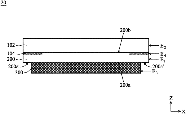
an anti-explosion layer disposed between the substrate and the display, wherein the anti-explosion layer has a tensile strength, and the tensile strength is in a range from 10 MPa to 30 MPa,
wherein the anti-explosion layer has a first side and the substrate has a second side, and a distance between the first side and the second side is in a range from 0 mm to 0.3 mm,
wherein the anti-explosion layer is in contact with the display and the substrate, the display is adhered to the substrate through the anti-explosion layer, and the anti-explosion layer has a peel adhesion, and the peel adhesion is in a range from 40 N/mm to 150 N/mm, wherein the anti-explosion layer comprises a first surface, a portion of the first surface is in contact with the display and another portion of the first surface is not in contact with the display has a roughness, and the roughness (Ry) is in a range from 10 μm to 40 μm.
|