| CPC B24B 37/005 (2013.01) [B24B 37/013 (2013.01); B24B 49/105 (2013.01); H01L 21/3212 (2013.01)] | 18 Claims |
|
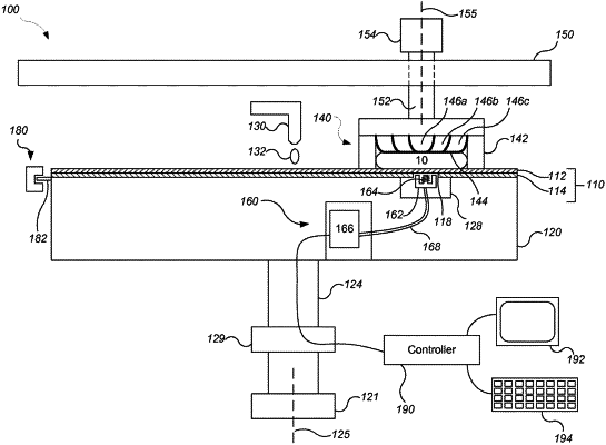
17. A polishing system, comprising:
a platen to support a polishing pad;
a carrier head to hold a substrate;
a motor to generate relative motion between the platen and the carrier head;
an in-situ eddy current monitoring system to monitor the substrate during polishing of the substrate; and
a controller configured to:
receive from a sensor of the in-situ eddy current monitoring system a sequence of signal values for a substrate being polished on the polishing pad;
calculate a sequence of thickness values from the sequence of signal values using a correlation curve;
repeatedly calculate a polishing rate from the sequence of thickness values during polishing of the substrate on the polishing pad;
for an initial time period during the polishing, calculate one or more first adjustments for one or more polishing parameters based on a current polishing rate using a first control algorithm;
detect a change in the polishing rate that meets at least one first predetermined criterion that indicates exposure of an underlying conductive layer in a stack of adjacent conductive layers on the substrate that is being polished; and
for a subsequent time period during the polishing and after detection of the change in the polishing rate, calculate one or more second adjustments for one or more polishing parameters based on the polishing rate using a different second control algorithm, wherein calculating the sequence of thickness values use the correlation curve based on a resistivity of a same layer from the stack of adjacent conductive layers during the initial time period and the subsequent time period.
|