| CPC B23K 3/08 (2013.01) [B23K 1/085 (2013.01); B23K 3/0653 (2013.01); B23K 3/087 (2013.01); B29C 64/106 (2017.08); B29C 64/112 (2017.08); B29C 64/393 (2017.08); B33Y 50/02 (2014.12); B33Y 80/00 (2014.12); H05K 3/3447 (2013.01); H05K 3/3468 (2013.01); H05K 13/0465 (2013.01); B29L 2031/3425 (2013.01); B29L 2031/7178 (2013.01); B33Y 10/00 (2014.12); H05K 2203/0165 (2013.01); H05K 2203/0173 (2013.01); H05K 2203/044 (2013.01)] | 5 Claims |
|
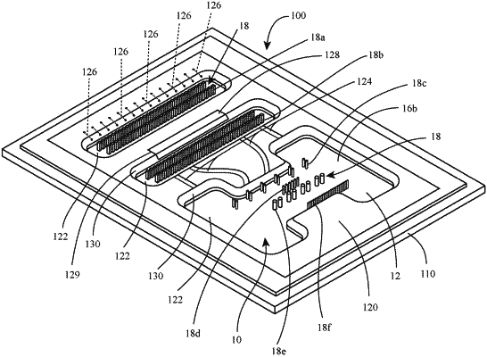
1. A method of manufacturing a printed circuit board assembly, the method comprising:
providing a circuit board;
determining a solder flow for the circuit board;
supporting the circuit board on a pallet, the pallet including an inner body comprising at least one opening for receiving solder flow and geometries to achieve the determined solder flow,
the geometries of the inner body including one or more of tunnels in fluid communication with a lower surface of the pallet and the at least one opening, a plurality of channels defined through the lower surface of the pallet and in fluid communication with the at least one opening, at least one ramp seated within a recess defined within the inner body, wherein the at least one ramp is in fluid communication with the at least one opening;
positioning a plurality of components on the circuit board, the plurality of components including a plurality of lead pins extending through the circuit board and protruding from an underside of the circuit board and at least partially through the at least one opening defined within the pallet; and
passing the pallet through a wave solder machine such that molten solder contacts the pallet and the geometries of the pallet control the molten solder to flow according to the determined solder flow to establish connections between the plurality of lead pins.
|