| CPC B06B 1/0607 (2013.01) [B06B 1/067 (2013.01); G01D 5/62 (2013.01); G06F 3/043 (2013.01); B06B 2201/55 (2013.01)] | 19 Claims |
|
1. A piezoelectric sensor assembly, comprising:
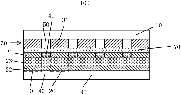
a base substrate;
a plurality of ultrasonic transducers, wherein a spacing area is provided between two adjacent ultrasonic transducers; and
an acoustic matching layer, wherein the acoustic matching layer comprises a plurality of acoustic matching areas, and an orthographic projection of at least one acoustic matching area on the base substrate falls into an orthographic projection of the ultrasonic transducer corresponding to the acoustic matching area on the base substrate,
wherein an isolation cavity is provided between two adjacent acoustic matching areas; and
wherein the piezoelectric sensor further comprises: a pore layer on a side of the acoustic matching layer away from the base substrate.
|