| CPC H05K 1/0393 (2013.01) [G02F 1/133308 (2013.01); G02F 1/133608 (2013.01); H05K 3/24 (2013.01); H05K 3/4652 (2013.01)] | 14 Claims |
|
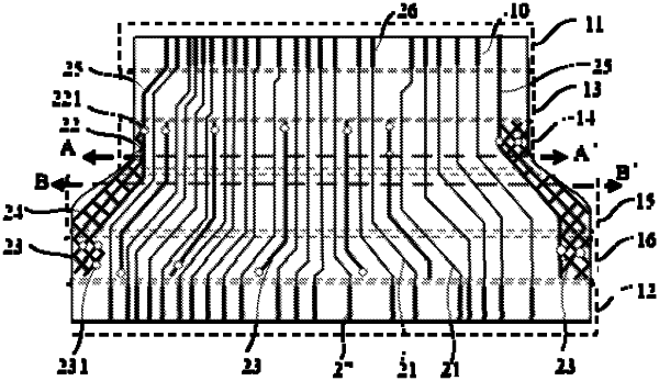
1. A flexible printed circuit, comprising a flexible substrate, wherein the flexible substrate is divided into wiring areas, a first bonding area and a second bonding area which are located on two sides of the wiring areas, and the wiring areas comprise a first wiring area, a second wiring area, a third wiring area and a fourth wiring which are away from the first bonding area in sequence;
the flexible printed circuit further comprises a wiring layer arranged on the flexible substrate and a reinforcing layer arranged on a side of the flexible substrate away from the wiring layer;
the wiring layer comprises a plurality of signal wirings arranged along the first wiring area, the second wiring area, the third wiring area and the fourth wiring area, and the reinforcing layer comprises a first reinforcing structure located in the second wiring area and a second reinforcing structure located in the fourth wiring area;
the flexible printed circuit further comprises a third reinforcing structure and a fourth reinforcing structure which are arranged on a same layer as the signal wirings, the third reinforcing structure is located in the second wiring area, the fourth reinforcing structure is located in the fourth wiring area, and orthographic projections of the third reinforcing structure and the fourth reinforcing structure on the flexible substrate are not superimposed with orthographic projections of the signal wirings on the flexible substrate;
the third reinforcing structure is connected to the first reinforcing structure through a first via hole that penetrates through the flexible substrate, and the fourth reinforcing structure is connected to the second reinforcing structure through a second via hole that penetrates through the flexible substrate;
the flexible printed circuit further comprises a fifth reinforcing structure arranged on a same layer as the signal wirings, wherein the fifth reinforcing structure is located in the third wiring area, and an orthographic projection of the fifth reinforcing structure on the flexible substrate is not superimposed with orthographic projections of the signal wirings on the flexible substrate; and
the fifth reinforcing structure is respectively connected to the third reinforcing structure and the fourth reinforcing structure.
|