| CPC H05K 1/0284 (2013.01) [B29C 45/14 (2013.01); B29C 45/26 (2013.01); H01L 33/64 (2013.01); H05K 1/02 (2013.01); H05K 1/0203 (2013.01); H05K 1/05 (2013.01); H05K 1/11 (2013.01); H05K 1/183 (2013.01); H05K 3/0014 (2013.01); H05K 3/185 (2013.01); B29L 2031/3425 (2013.01); B29L 2031/747 (2013.01); H05K 2201/0129 (2013.01); H05K 2201/10106 (2013.01)] | 9 Claims |
|
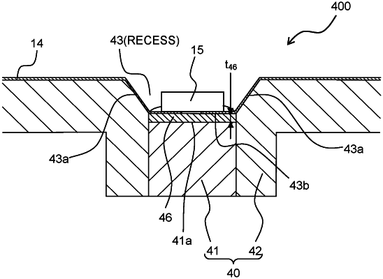
1. A three-dimensional molded circuit component, comprising:
a base member which includes a metal part and a resin part;
a circuit pattern which is formed on the resin part;
a resin thin film which is formed on the metal part, and which includes one of a thermosetting resin and a photo-curable resin; and
a mounted component which is mounted on the resin thin film, and is electrically connected to the circuit pattern, wherein
the resin thin film has a first surface and a second surface opposing each other, the first surface of the resin thin film is formed on the metal part, and the second surface of the resin thin film is formed with a part of the circuit pattern, on which the mounted component is disposed,
the mounted component is electrically connected, by a solder, to the part of the circuit pattern formed on the second surface of the resin thin film,
on the base member, a recess is defined by a side wall formed by the resin part and a base formed by the resin thin film, the mounted component is mounted in the recess,
a thickness of the resin thin film is in the range of 0.01 mm to 0.5 mm, and
the resin thin film is not a portion of the resin part and is a separate member from the resin part.
|