| CPC H05K 1/0251 (2013.01) [G01R 1/07342 (2013.01); H05K 1/115 (2013.01); H05K 1/118 (2013.01)] | 14 Claims |
|
1. A trace embedded probe device comprising:
a circuit board comprising:
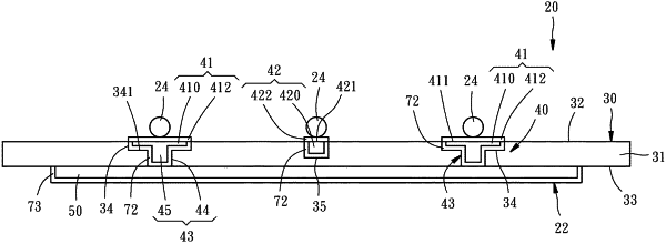
an insulating layer unit having an upper surface, a lower surface, and two first recesses and a second recess, which are recessed from the upper surface, the second recess being located between the two first recesses;
two grounding traces each comprising a trace main body, the trace main bodies of the two grounding traces being disposed in the two first recesses respectively in a way that the trace main bodies of the two grounding traces are flush in elevation with the upper surface of the insulating layer unit;
a signal trace comprising a trace main body, the trace main body of the signal trace being disposed in the second recess in a way that the trace main body of the signal trace is flush in elevation with the upper surface of the insulating layer unit;
a grounding layer disposed on the lower surface of the insulating layer unit; and
a plurality of conductive vias arranged in a way that the trace main body of each of the grounding traces being connected with the grounding layer by at least one of the conductive vias, each of the conductive vias comprising a through hole penetrating through an inner bottom surface of the first recess and the lower surface of the insulating layer unit, and a conductive layer disposed in the through hole;
wherein the trace main bodies of the grounding traces, the trace main body of the signal trace, the grounding layer and the conductive layers of the conductive vias are made of a same metal material; and
three probes disposed on the grounding traces and the signal trace, respectively.
|