| CPC H03K 5/135 (2013.01) [G06F 1/04 (2013.01); G06F 30/392 (2020.01); H03K 3/037 (2013.01); H03K 17/6872 (2013.01); G06F 2117/04 (2020.01)] | 20 Claims |
|
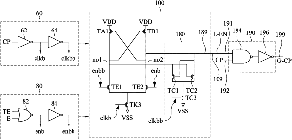
1. An integrated circuit comprising:
a clocking transistor having a gate terminal configured to receive a first clock signal;
a first enabling transistor having a semiconductor channel electrically connected between a drain terminal of the clocking transistor and a first node, wherein the first enabling transistor has a gate terminal configured to receive a first enabling signal;
a second enabling transistor having a semiconductor channel electrically connected between a drain terminal of the clocking transistor and a second node, wherein the second enabling transistor has a gate terminal configured to receive a second enabling signal which is a logic inverse of the first enabling signal;
a branch-one transistor having a semiconductor channel electrically connected between a first power supply and the first node and having a gate terminal electrically connected to the second node, wherein a source terminal of the branch-one transistor is configured to be maintained at a constant supply voltage on the first power supply, wherein the clocking transistor has a source terminal electrically connected to a second power supply;
a branch-two transistor having a semiconductor channel electrically connected between the first power supply and the second node and having a gate terminal electrically connected to the first node, wherein a source terminal of the branch-two transistor is configured to be maintained at the constant supply voltage on the first power supply;
a clock gating circuit having an output terminal configured to generate a gated clock signal and having a first input terminal configured to receive a latch output signal which is latched to a logic level of either a first node signal at the first node or a second node signal at the second node; and
a coupling circuit configured to generate the latch output signal from at least one of the first node signal at the first node or the second node signal at the second node.
|