| CPC H03K 19/1958 (2013.01) [G06F 1/0321 (2013.01); G06F 9/30098 (2013.01); G06F 9/4498 (2018.02); G06N 10/00 (2019.01); G11C 11/44 (2013.01); H02M 1/08 (2013.01); H02M 3/07 (2013.01); H03K 19/195 (2013.01); H10B 63/30 (2023.02)] | 19 Claims |
|
1. A system for controlling qubit gates comprising:
a first packaged device comprising a quantum device including a plurality of qubit gates, wherein the quantum device is configured to operate at a cryogenic temperature; and
a second packaged device comprising a control system configured to operate at the cryogenic temperature, wherein the first packaged device is coupled to the second packaged device, and wherein the control system comprises:
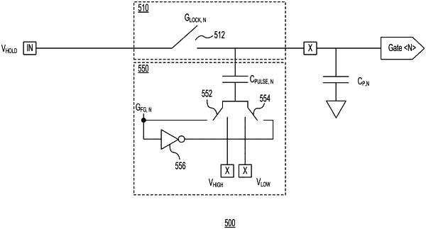
a plurality of charge locking circuits, wherein each of the plurality of charge locking circuits is coupled to at least one qubit gate of the plurality of qubit gates via an interconnect such that each of the plurality of charge locking circuits is configured to provide a voltage signal to at least one qubit gate, and
a control circuit comprising a finite state machine configured to provide at least one control signal to selectively enable at least one of the plurality of charge locking circuits and to selectively enable a provision of at least one voltage signal to a selected one of the plurality of charge locking circuits, wherein each of the plurality of charge locking circuits further comprises a capacitor having a first terminal for receiving an input voltage signal and a second terminal for selectively receiving a first voltage amount or a second voltage amount.
|