| CPC H03K 17/223 (2013.01) [H03K 17/693 (2013.01)] | 11 Claims |
|
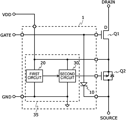
1. A semiconductor device that normally-off drives a first transistor that normally-on drives, the semiconductor device comprising:
a first circuitry that is connected with a power supply voltage terminal and a ground, detects the power supply voltage, and outputs a transition state of the power supply voltage;
a second circuitry that is connected with the power supply voltage terminal, the ground, the first circuitry, and a second transistor, and outputs a drive voltage of the second transistor connected in series with the first transistor, based on an output of the first circuitry; and
a first diode having an anode connected with a drive terminal of the first transistor and a cathode connected with an output terminal of the second transistor, wherein
the first circuitry comprises:
a reference voltage generation circuitry that generates a reference voltage; and
a voltage comparison circuitry that compares the reference voltage with the power supply voltage terminal; and
the second circuitry comprises:
an output buffer that controls an output of the voltage comparison circuitry to apply the output to a gate of the second transistor.
|