| CPC H01S 5/022 (2013.01) [H01S 5/0262 (2013.01); H01S 5/02461 (2013.01)] | 15 Claims |
|
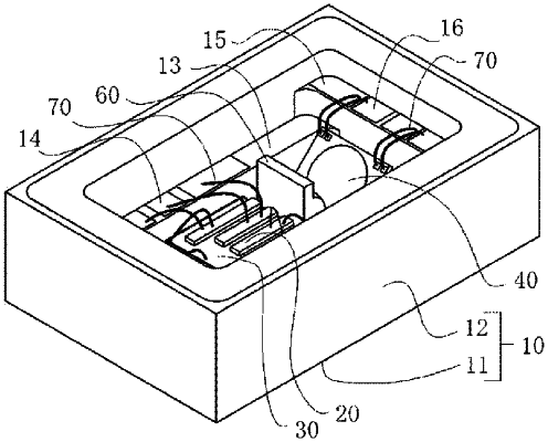
1. A light emitting device comprising:
a base having a bottom face and a lateral part surrounding the bottom face and extending upwards from the bottom face, wherein the lateral part has an uppermost face and comprises a first stepped portion including a first upper face and a second stepped portion including a second upper face and facing the first stepped portion, wherein the first upper face and the second upper face are disposed below the uppermost face, wherein the first upper face and the second upper face are disposed inward of the uppermost face in a top view, and wherein a height of the first stepped portion from the bottom face is different from a height of the second stepped portion from the bottom face;
a first semiconductor laser element disposed on the bottom face and located between the first stepped portion and the second stepped portion in a top view, wherein the first semiconductor laser element is configured to emit light towards the second stepped portion;
a first wiring region located on the first stepped portion; and
one or more first wires, each having a first end that is connected to the first wiring region, wherein:
at least one of the one or more first wires is electrically connected to the first semiconductor laser element.
|