| CPC H01R 12/716 (2013.01) [H01R 13/424 (2013.01)] | 6 Claims |
|
1. A board connector to be mounted on a circuit board, comprising:
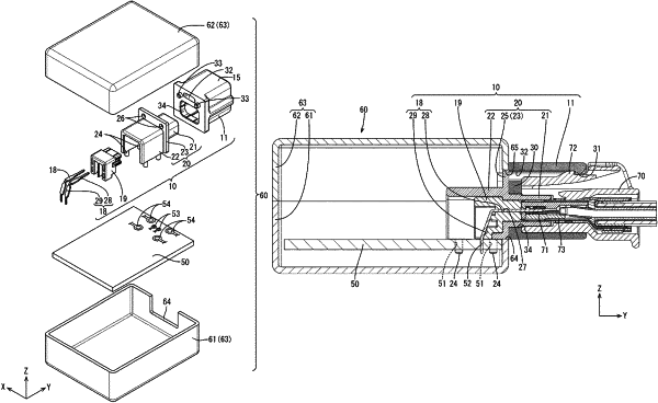
a connector housing including a receptacle having an opening facing a front direction and a back wall facing a rear direction and provided on a side opposite to the opening of the receptacle, the back wall including an outer conductor mounting hole and a through hole;
a mating connector configured to fit into the receptacle;
an outer conductor inserted in the outer conductor mounting hole to penetrate through the back wall;
an insulating dielectric disposed inside the outer conductor; and
an inner conductor disposed inside the dielectric,
wherein the outer conductor includes a flange configured to contact the back wall, the flange including a closing portion for closing the through hole, the through hole being formed at a position of the back wall different from the outer conductor mounting hole.
|