| CPC H01Q 1/2283 (2013.01) [H01L 23/3114 (2013.01); H01L 23/66 (2013.01); H05K 1/0237 (2013.01); H01L 2223/6677 (2013.01)] | 23 Claims |
|
1. An apparatus, comprising:
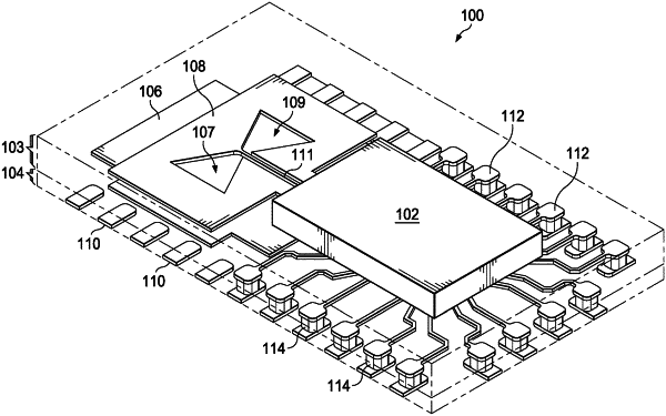
an antenna formed in a first conductor layer on a device side surface of a multilayer package substrate, the multilayer package substrate comprising conductor layers spaced from one another by dielectric material and coupled to one another by conductive vertical connection layers, the multilayer package substrate having a board side surface opposite the device side surface; and
a semiconductor die mounted to the device side surface of the multilayer package substrate spaced from and coupled to the antenna; wherein the bowtie antenna further comprises a first bow and a second bow formed as openings in the first conductor layer, the first bow and the second bow oriented to face in opposite directions, and a feed input comprising slots in the first conductor layer coupled to the first bow and the second bow.
|