| CPC H01L 31/02363 (2013.01) [H01L 31/048 (2013.01)] | 20 Claims |
|
1. A photovoltaic cell comprising:
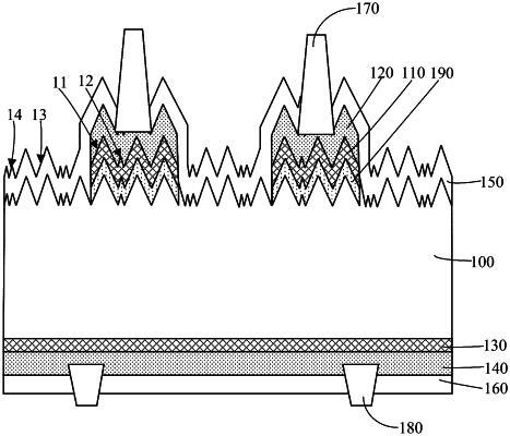
a substrate, wherein the substrate has a front surface with a plurality of metal pattern regions and a plurality of non-metal pattern regions;
a plurality of first pyramid structures and a plurality of second pyramid structures disposed in each of the plurality of metal pattern regions, wherein a dimension of a bottom portion of each of the plurality of first pyramid structures is greater than a dimension of a bottom portion of each of the plurality of second pyramid structures;
a plurality of third pyramid structures and a plurality of fourth pyramid structures disposed in each of the plurality of non-metal pattern regions, wherein a dimension of a bottom portion of each of the plurality of third pyramid structures is greater than a dimension of a bottom portion of each of the plurality of fourth pyramid structures; and wherein an area proportion of the plurality of first pyramid structures on a portion of the front surface of the substrate in a respective metal pattern region is greater than an area proportion of the plurality of third pyramid structures on a portion of the front surface of the substrate in a respective non-metal pattern region;
a first tunneling layer and a first doped conductive layer stacked on the portion of the front surface of the substrate in the respective metal pattern region in a direction away from the substrate; and
a second tunneling layer and a second doped conductive layer stacked on a rear surface of the substrate in a direction away from the substrate.
|