| CPC H01L 29/152 (2013.01) [H01L 29/66477 (2013.01); H01L 29/7849 (2013.01)] | 21 Claims |
|
1. A semiconductor device comprising:
a semiconductor layer; and
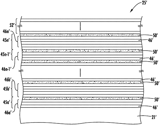
a superlattice adjacent the semiconductor layer and comprising a plurality of stacked groups of layers, each group of layers comprising a plurality of stacked base semiconductor monolayers defining a base semiconductor portion, and at least one non-semiconductor monolayer constrained within a crystal lattice of adjacent base semiconductor portions;
the at least one non-semiconductor monolayer in a first group of layers of the superlattice comprising oxygen and devoid of carbon, and the at least one non-semiconductor monolayer in a second group of layers of the superlattice comprising carbon, the second group of layers being above the first group of layers in the superlattice.
|