| CPC H01L 27/156 (2013.01) [H01L 33/005 (2013.01); H01L 33/12 (2013.01); H01L 33/38 (2013.01); H01L 33/54 (2013.01); H01L 33/62 (2013.01); H01L 2933/005 (2013.01); H01L 2933/0016 (2013.01); H01L 2933/0066 (2013.01)] | 19 Claims |
|
1. A display panel comprising:
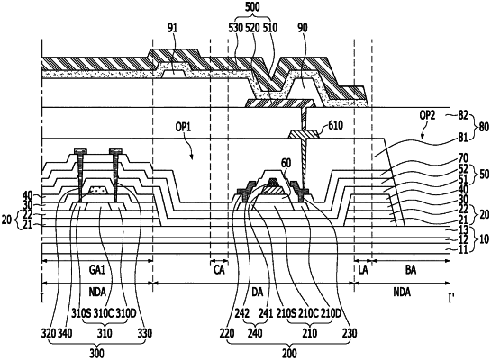
a substrate comprising a display area that includes a plurality of sub-pixels, and a non-display area disposed adjacent to the display area, the non-display area including a gate driving area comprising a gate driving circuit and a bending area disposed outside the display area and the gate driving area;
a first buffer layer contacting the substrate in the gate driving area, the first buffer layer including a first lower opening in the display area and a second lower opening in the bending area;
a second buffer layer contacting the display area of the substrate exposed by the first lower opening of the first buffer layer, the second buffer layer including an upper opening in the bending area;
a first thin film transistor disposed on the second buffer layer in the display area, the first thin film transistor comprising a first semiconductor layer made of a first semiconductor; and
a second thin film transistor disposed on the first buffer layer in the gate driving area, the second thin film transistor comprising a second semiconductor layer made of a second semiconductor different from the first semiconductor,
wherein the first thin film transistor overlaps the first lower opening of the first buffer layer,
wherein the upper opening is disposed in the second lower opening, such that an end of the first buffer layer disposed in the bending area is covered by the second buffer layer.
|