| CPC H01L 27/1469 (2013.01) [H01L 21/311 (2013.01); H01L 23/481 (2013.01); H01L 23/485 (2013.01); H01L 23/488 (2013.01); H01L 23/49827 (2013.01); H01L 27/148 (2013.01); H01L 27/1462 (2013.01); H01L 27/14632 (2013.01); H01L 27/14634 (2013.01); H01L 27/14636 (2013.01); H01L 27/14685 (2013.01); H04N 25/75 (2023.01)] | 8 Claims |
|
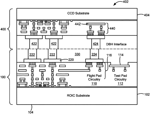
1. An assembly including first and second wafers directly bonded to each other, comprising:
direct bonding posts electrically connecting the first and second wafers;
an oxide layer on direct bonding sides of the first and second wafers; and
a direct bonding interface at bonding surfaces of the first and second wafers, wherein the assembly includes a backside surface and a frontside surface, the first wafer includes IO signal connections vertically routed to the direct bonding interface by a first one of the bonding posts on the first wafer bonded to a first one of the bonding posts on the second wafer, and the second wafer comprises vertical routing of the IO signal connections from first one of the bonding posts on the second wafer to IO pads on a backside surface of the assembly.
|