| CPC H01L 27/1203 (2013.01) [H01L 21/84 (2013.01); H01L 27/092 (2013.01); H01L 29/045 (2013.01); H01L 27/0688 (2013.01)] | 14 Claims |
|
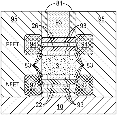
1. A semiconductor device comprising:
a semiconductor substrate with a first crystalline surface orientation;
a first type field-effect transistor directly on the semiconductor substrate and directly under a dielectric material contacting a second type field-effect transistor, wherein the first type field-effect transistor with the first crystalline surface orientation in a first plurality of nanosheet channels; and
the second type field-effect transistor directly on the dielectric material with a second crystalline surface orientation in a second plurality of nanosheet channels, wherein the second plurality of nanosheet channels are parallel to the semiconductor substrate.
|