| CPC H01L 27/0255 (2013.01) [H01L 29/1608 (2013.01)] | 7 Claims |
|
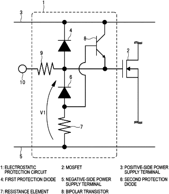
1. A semiconductor device comprising:
an electrostatic protection circuit; and
a MOSFET including a gate terminal, wherein
the electrostatic protection circuit includes
a positive-side first power supply terminal,
a negative-side second power supply terminal,
a first protection diode including a first cathode terminal electrically connected to the first power supply terminal and a first anode terminal electrically connected to the gate terminal,
a second protection diode including a second anode terminal electrically connected to the second power supply terminal via a first resistance element, and a second cathode terminal electrically connected to the gate terminal, and
a bipolar transistor including a base terminal, an emitter terminal, and a collector terminal,
wherein the first protection diode, the second protection diode, the bipolar transistor, and the first resistance element are respectively formed on a semiconductor substrate made of silicon carbide, and
the bipolar transistor is electrically connected to the second anode terminal, the gate terminal, and the first power supply terminal.
|