| CPC H01L 25/18 (2013.01) [H01L 24/83 (2013.01); H01L 25/50 (2013.01); H10B 12/036 (2023.02); H10B 12/33 (2023.02); H10B 12/482 (2023.02); H10B 12/485 (2023.02); H10B 12/488 (2023.02); H01L 2224/83895 (2013.01); H01L 2224/83896 (2013.01)] | 13 Claims |
|
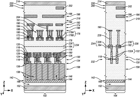
1. A microelectronic device, comprising:
array regions individually comprising:
memory cells comprising access devices and storage node devices;
digit lines coupled to the access devices and extending in a first direction;
word lines coupled to the access devices and extending in a second direction orthogonal to the first direction; and
control logic devices over and in electrical communication with the memory cells;
digit line exit regions horizontally alternating with the array regions in the first direction and individually comprising:
portions of the digit lines extending beyond the array regions adjacent thereto;
digit line contact structures extending through at least some of the portions of the digit lines;
metallic interconnect structures on the digit line contact structures and individually comprising:
a vertical contact region comprising a first portion of a metal material; and
a horizontal pad region overlying the vertical contact region and having greater horizontal dimensions than the vertical contact region, the horizontal pad region comprising:
a first additional portion of the metal material integral and continuous with the first portion of the metal material; and
a first further portion of the metal material overlying and bonded to the first additional portion of the metal material;
contact structures on the metallic interconnect structures; and
routing structures coupled to the contact structures;
word line exit regions horizontally alternating with the array regions in the second direction and individually comprising:
portions of the word lines extending beyond the array regions adjacent thereto;
word line contact structures extending through at least some of the portions of the word lines;
additional metallic interconnect structures on the word line contact structures and individually comprising:
an additional vertical contact region comprising a second portion of the metal material; and
an additional horizontal pad region overlying the additional vertical contact region and having greater horizontal dimensions than the additional vertical contact region, the additional horizontal pad region comprising:
a second additional portion of the metal material integral and continuous with the second portion of the metal material; and
a second further portion of the metal material overlying and bonded to the second additional portion of the metal material;
additional contact structures on the additional metallic interconnect structures; and
additional routing structures coupled to the additional contact structures.
|