| CPC H01L 25/0657 (2013.01) [H01L 25/18 (2013.01); H01L 2225/0651 (2013.01); H01L 2225/06506 (2013.01); H01L 2225/06562 (2013.01)] | 16 Claims |
|
1. An apparatus, comprising:
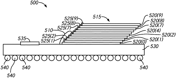
a plurality of memory devices including first, second, and third memory devices, the first memory device including a first bond pad, the second memory device including a second bond pad, the third memory device including a third bond pad, the second memory device disposed between the first and third memory devices;
a first conductor coupled to the first bond pad of the first memory device and the second bond pad of the second memory device;
a second conductor coupled to the second bond pad of the second memory device and the third bond pad of the third memory device; and
a source conductor coupled to the second bond pad and at least one conductive signal line, the source conductor being configured to provide a signal to the second bond pad, wherein the first conductor provides the signal from the second bond pad to the first bond pad with a first signal timing and the second conductor provides the signal from the second bond pad to the third bond pad with a second signal timing equal to the first signal timing, wherein no source conductor directly couples the at least one conductive signal line to the first bond pad or the third bond pad, and wherein the first memory device is limited to receiving the signal at the first bond pad through the first conductor from the second bond pad and the third memory device is limited to receiving the signal at the third bond pad through the second conductor from the second bond pad.
|