| CPC H01L 23/66 (2013.01) [H01L 24/49 (2013.01); H01L 29/2003 (2013.01); H01L 29/41775 (2013.01); H01L 29/7786 (2013.01); H01L 2223/6611 (2013.01); H01L 2223/6616 (2013.01); H01L 2223/6655 (2013.01); H01L 2223/6683 (2013.01); H01L 2224/49107 (2013.01); H01L 2924/13064 (2013.01); H01L 2924/1421 (2013.01); H01L 2924/30111 (2013.01)] | 20 Claims |
|
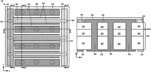
1. A radio frequency (“RF”) amplifier, comprising:
a Group III nitride-based RF amplifier die that includes a semiconductor layer structure and a gate terminal, a source terminal and a drain terminal on the semiconductor layer structure,
wherein a plurality of unit cell transistors are provided in an upper portion of the semiconductor layer structure, and at least two of the gate terminal, the drain terminal and the source terminal are provided on a lower surface of the semiconductor layer structure,
wherein at least one of the gate terminal and the drain terminal is electrically connected to the unit cell transistors through a conductive via, and
wherein an inductance of the conductive via comprises at least a portion of a matching circuit.
|