| CPC H01L 23/5389 (2013.01) [H01L 21/486 (2013.01); H01L 21/4846 (2013.01); H01L 21/4853 (2013.01); H01L 21/565 (2013.01); H01L 21/568 (2013.01); H01L 21/6835 (2013.01); H01L 23/3114 (2013.01); H01L 23/3128 (2013.01); H01L 23/49811 (2013.01); H01L 23/49827 (2013.01); H01L 23/50 (2013.01); H01L 23/5383 (2013.01); H01L 23/66 (2013.01); H01L 25/0657 (2013.01); H01L 25/10 (2013.01); H01L 25/105 (2013.01); H01L 25/16 (2013.01); H01L 25/162 (2013.01); H01L 25/165 (2013.01); H01L 25/50 (2013.01); H01Q 1/2283 (2013.01); H01Q 9/0407 (2013.01); H01Q 9/0414 (2013.01); H01L 23/145 (2013.01); H01L 23/49816 (2013.01); H01L 24/13 (2013.01); H01L 24/16 (2013.01); H01L 24/48 (2013.01); H01L 24/81 (2013.01); H01L 2221/68345 (2013.01); H01L 2221/68359 (2013.01); H01L 2223/6677 (2013.01); H01L 2224/131 (2013.01); H01L 2224/13101 (2013.01); H01L 2224/16225 (2013.01); H01L 2224/16227 (2013.01); H01L 2224/16238 (2013.01); H01L 2224/45099 (2013.01); H01L 2224/48227 (2013.01); H01L 2224/81005 (2013.01); H01L 2225/1023 (2013.01); H01L 2225/1041 (2013.01); H01L 2225/1058 (2013.01); H01L 2924/00014 (2013.01); H01L 2924/014 (2013.01); H01L 2924/1533 (2013.01); H01L 2924/1579 (2013.01); H01L 2924/15311 (2013.01); H01L 2924/181 (2013.01); H01L 2924/19041 (2013.01); H01L 2924/19042 (2013.01); H01L 2924/19043 (2013.01); H01L 2924/19106 (2013.01); H01Q 21/065 (2013.01)] | 19 Claims |
|
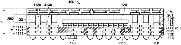
1. A semiconductor package, comprising:
a first substrate;
a first layer structure;
a second layer structure; and
a first antenna layer formed on at least one of the first layer structure and the second layer structure, wherein the first antenna layer has an upper surface flush with a layer upper surface of the first layer structure or the second layer structure;
wherein the first layer structure is formed between the first substrate and the second layer structure, and wherein the first layer structure comprises a second substrate and a first package body, the second substrate has a receiving portion including an electronic component, and the first package body fills up the receiving portion, the first package body encapsulating the electronic component.
|