| CPC H01L 23/49513 (2013.01) [H01L 21/563 (2013.01); H01L 21/565 (2013.01); H01L 23/3114 (2013.01); H01L 23/4952 (2013.01); H01L 23/49548 (2013.01); H01L 24/09 (2013.01); H01L 24/17 (2013.01); H01L 24/32 (2013.01); H01L 24/49 (2013.01); H01L 24/73 (2013.01); H01L 2924/1304 (2013.01); H01L 2924/141 (2013.01)] | 16 Claims |
|
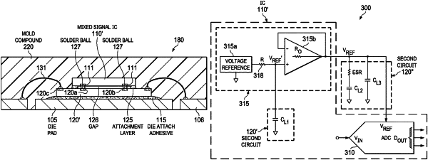
1. A semiconductor device assembly method, comprising:
mounting a first circuit on a die pad of a leadframe, the first circuit having a region;
mounting a second circuit on the first circuit via interconnects, in which the region is spaced from the second circuit by a gap and by the interconnects;
forming an attachment layer between the first and second circuits and around the interconnects, in which the attachment layer and the first and second circuits enclose at least a part of the gap over the region; and
encapsulating the first and second circuits, the attachment layer, and the at least part of the gap by a mold compound.
|