| CPC H01L 23/49513 (2013.01) [H01L 21/4825 (2013.01); H01L 23/3121 (2013.01); H01L 23/49562 (2013.01); H01L 24/03 (2013.01); H01L 24/08 (2013.01); H01L 24/48 (2013.01); H01L 29/407 (2013.01); H01L 29/41766 (2013.01); H01L 29/7396 (2013.01); H01L 29/7397 (2013.01); H01L 29/7802 (2013.01); H01L 29/7813 (2013.01); H01L 29/8611 (2013.01); H01L 2224/022 (2013.01); H01L 2224/0219 (2013.01); H01L 2224/02185 (2013.01); H01L 2224/03011 (2013.01); H01L 2224/04034 (2013.01); H01L 2224/04042 (2013.01); H01L 2224/0603 (2013.01); H01L 2224/48111 (2013.01); H01L 2224/48237 (2013.01); H01L 2224/4903 (2013.01); H01L 2224/49111 (2013.01); H01L 2224/84815 (2013.01); H01L 2224/8592 (2013.01); H01L 2224/85815 (2013.01)] | 20 Claims |
|
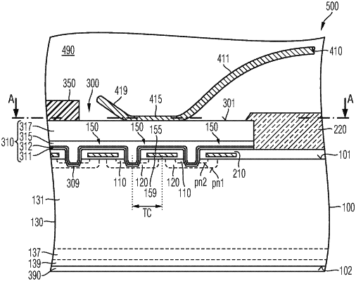
1. A method of manufacturing a semiconductor device, the method comprising:
forming a base portion of a bonding pad on a semiconductor portion, the base portion further comprising a base layer;
forming a main surface of the bonding pad, the main surface comprising a bonding region;
bonding a bond wire or clip to the bonding region; and
forming a supplemental structure directly on the base portion, wherein the supplemental structure laterally adjoins the bond wire or clip or is laterally spaced apart from the bond wire or clip, and wherein a volume-related specific heat capacity of the supplemental structure is higher than a volume-related specific heat capacity of the base layer.
|