| CPC H01L 23/3185 (2013.01) [H01L 21/561 (2013.01); H01L 21/568 (2013.01); H01L 21/78 (2013.01); H01L 23/3171 (2013.01); H01L 23/552 (2013.01); H01L 21/6836 (2013.01); H01L 2221/68336 (2013.01)] | 19 Claims |
|
1. A chip scale package (CSP), comprising:
a semiconductor die;
a conductive terminal coupled to the semiconductor die; and
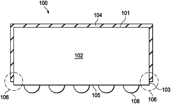
a non-conductive coat including a top portion covering a backside of the semiconductor die and a sidewall portion covering a sidewall of the semiconductor die, the non-conductive coat having a thickness of less than 45 microns, the sidewall portion of the non-conductive coat having a uniform thickness on the sidewall of the semiconductor die and the top portion having a width corresponding to a sum of a width of the semiconductor die and twice of the uniform thickness of the sidewall portion, wherein a strip of the sidewall of the semiconductor die is exposed and the sidewall portion terminates at the strip of the sidewall, wherein the strip of the sidewall abuts a frontside of the semiconductor die opposite the backside.
|