| CPC H01L 23/31 (2013.01) [H01L 23/3677 (2013.01); H01L 23/49568 (2013.01)] | 16 Claims |
|
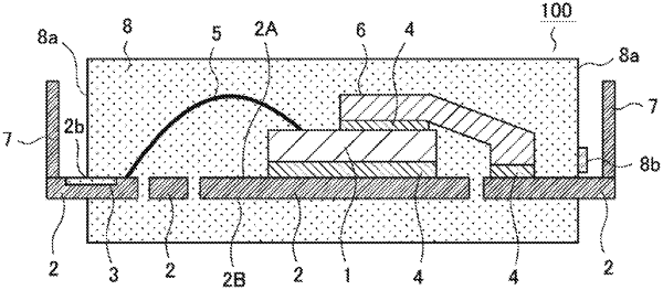
1. A semiconductor device comprising:
a mounting portion of a lead frame on which a semiconductor element is mounted and which is made of metal;
a heat dissipation portion opposite to the mounting portion; and
a resin sealing the mounting portion on which the semiconductor element is mounted and the heat dissipation portion, wherein
the lead frame has a scale-like portion on which scale-shaped projections are consecutively formed, and
the scale-like portion is provided over both sides across a resin boundary portion which is a boundary between inside and outside of an area sealed by the resin on the lead frame, wherein the scale-like portion is configured to provide a discharge path for a gas from the inside of the area to the outside of the area at a time of a molding of the resin to the lead frame.
|